High Power PCB
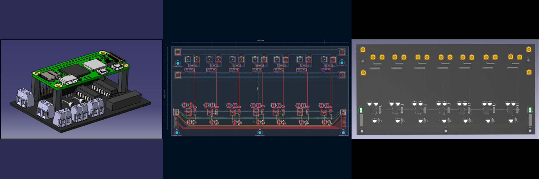
This is a long project breakdown and may read a little weird currently, I need to refine it.
A 3-board power electronics system (KiCad) driving a 14-winding test coil rig rated for 150A/200V, selecting and integrating isolated gate drivers, DC-DC isolation, and a 250V/240A power MOSFET stage to meet thermal (400°C) and vibration test requirements.
Project Overview
The task was to design and build a custom electronics system to drive a 14-winding test coil/rotor assembly for a thermal/mechanical test rig (test bed involves heating, shaking, and insulation testing). This is being designed in KiCad (electronics) and CATIA (mechanical/3D), as well as some future Ansys (thermal analysis).
Main Project Outline
- 14 windings, current applied in sequence to each winding within a controllable time domain, driven from a GUI.
- Power source: DC supply.
- Absolute maximums: ~150A current, ~200V.
- Cable size: >16mm², power flows through the cables for ~10 seconds.
- Thermal requirement: board must survive 400°C testing environment with cooling (aluminum heatsinking) and be able to withstand being shaken (vibration/shaker table).
- Circuit topology: MOSFET + gate driver per winding; gate driver connected to a microcontroller; MOSFET drain output connected to the winding. Board needs an ON/OFF signal pin on the gate driver connector.
- Control: system should be controllable from a PC via onboard Raspberry Pi with a web GUI.
- Preferred component suppliers: Conrad Elektronik, RS Components, Farnell (also Reichelt, Mouser used in practice).
System Architecture — Board Breakdown
The design has evolved into three separate boards:
- Power Electronics Board — MOSFETs, copper-pour power routing, thermal/heatsink design; this is the highest-complexity board.
- Communication Board — Raspberry Pi interface board; handles PC/GUI communication, connectors, pin header, schematic/routing for gate-driver signaling logic.
- Vibration Table Board — lighter schematic to connect signaling to the rotor/shaker table hardware.
Originally conceived as a single "Winding Board" containing all 14 sets of components, later split into multiple boards for isolation reasons.
Key Design Decisions & Component Choices
| Area | Decision / Current Status |
|---|---|
| Control | Considered Arduino vs. Raspberry Pi; settled on Raspberry Pi (moved from Pi Zero W → Raspberry Pi Pico at one point for the model). Physical stackup with Pi ≈ 18 mm with pin extenders; an 18 mm M3 spacer modeled in CATIA. |
| Pi/Board interconnect | 2.54mm 2x20 pin header/socket (Conrad "econ-connect" 1311390-62, Reichelt BKL 10120963). 40-pin connector option (Farnell 2213S-40G). PCB connector to Communication Board: Phoenix Contact MSTB 2,5/2-ST-5,08. |
| Bus/signaling | Two 8-bit sequencers with the Pi to transmit a 14-bit signal across windings with T/14 timing shift between each one. |
| Power relays for isolation / insulation | LEV200A4ANA. Physically separate from the actual Power Electronics Boards, acting as an isolation boundary. Handles connecting the 200V to the high power board. |
| High-power MOSFET | Landed on IXFK240N25X3 after a few iterations. Rated for 250V, 240A to handle any thermal derating. |
| Gate driver | Si8261ACD-C-IS. Gate input goes directly to this gate driver, which has internal isolation. Connects to the 12V DC/DC board. |
| DC-DC board | NXE2S1212MC. Isolates the 12V from the signal side to the high power side. |
| Gate drive voltage | Driving slightly below ideal (12V instead of 15V), but not an issue. |
| IDC signal connectors | Using the XG2A-1601 IDC connector for ribbon cables. Picked because it transmits up to 16 signals well. |
| PCB onboard heatsink | Fan/force-cooled aluminum heatsink. Currently working on finding an option that works. Ansys simulation planned for the newly selected heatsink. Isolation of heatsink from PCB is a shorting risk to manage carefully. |
| Copper bus bars | 1.5mm thick, minimum 10mm width for the high-current sections that will be laser cut. There are also copper pours that correspond to these bus bars for conduction. |
| Winding connectors | Iterated from generic connectors → screw terminals → heavy-duty screw terminals → Wurth Elektronik REDCUBE Press-Fit Screw Terminal 7461084. |
| Mounting/housing | Housing situation still open. |
| Mechanical (CATIA) | Spool + Bosch assembly attachment is an ongoing, not-yet-finished task. Mechanical design is done through CATIA. The KiCad files can be exported as .step files, however this can be quite difficult to edit afterwards. |
| Documentation | Documentation is done primarily through manual documents. |
Communication Board
Overview
This board is responsible for taking the program from the Raspberry Pi, running that data through two 8-bit sequencers to create 14 signals that are transmitted through a ribbon cable in order to turn each winding on/off.
Schematic
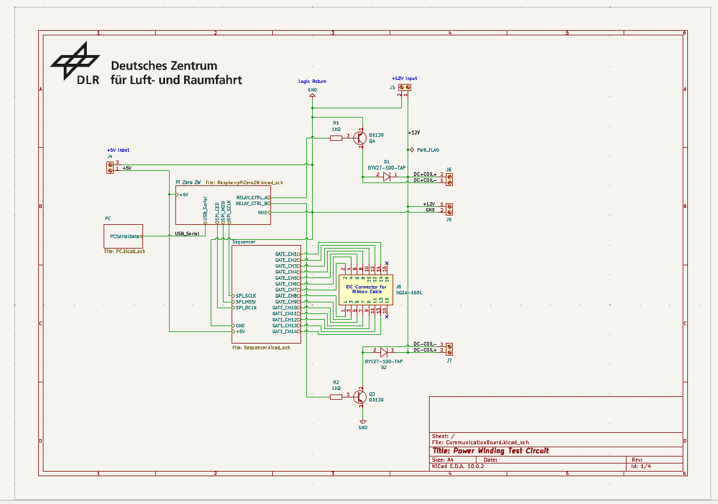
Figure 1 — Communication Board root schematic
The top-level schematic (the "root") outlines the screw terminals around the perimeter of the board, as well as the routing between the subcomponents and sub sheets. The Raspberry Pi outputs signals that turn on the relays that go through a transistor then through a diode to rectify the power breakdown. The following table outlines the purpose of each component at this view.
Table 1 — Component breakdown
| Component | Description / Purpose |
|---|---|
| BD139 (power transistor) | A power transistor that's activated by signals from the Raspberry Pi. |
| BYV27-100-TAP (freewheeling diode) | Acts as a barrier to prevent a voltage spike. |
| XG2A-1601 (IDC connector) | A PCB-mountable connector for a ribbon cable. |
| 398900302 (screw terminal) | PCB-mountable connectors for wires for connecting to external devices. |
| Raspberry Pi Pico (or Zero W) | An external device (microcontroller) that hosts a GUI that can be used with a computer. |
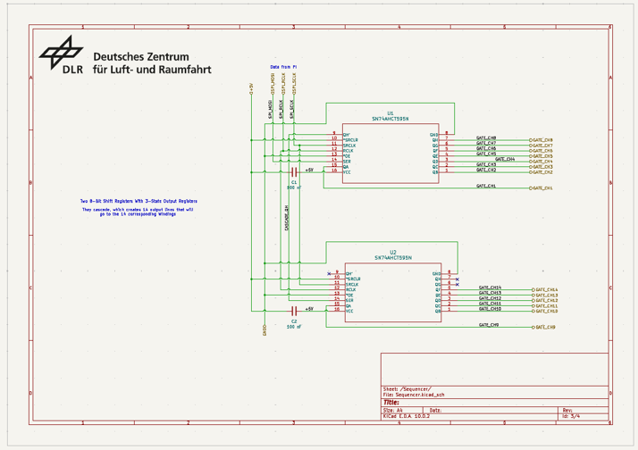
The sequencer sheet just highlights the signals that come from the Raspberry Pi, and then outputs 14 gate channel signals that are used to enable the power MOSFETs on the high power board. The capacitors before the VCC input pins are there from the datasheet.
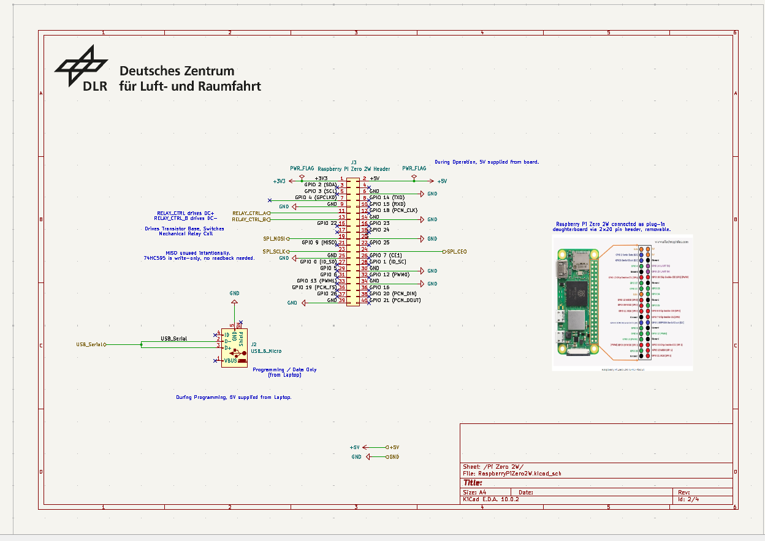
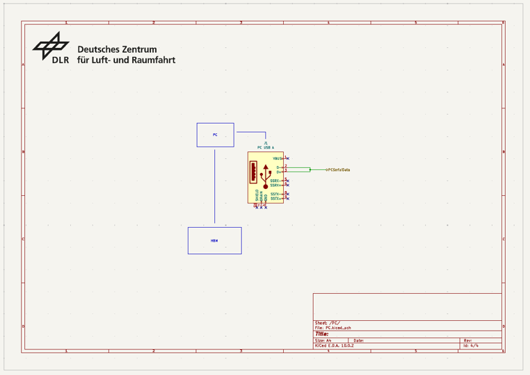
The PC and Raspberry Pi sub sheets are quite simple, but are there to represent how the Communication Board works with the other external components.
Footprints
Routing
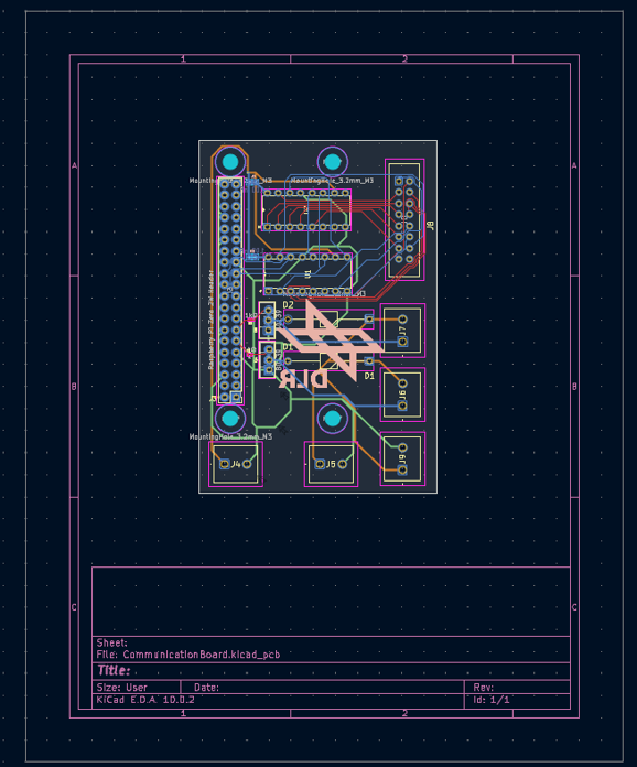
The board is routed with the ground and power layers in the middle, with the signal routing done on the top and bottom layers. The mounting holes are placed that way to overlay with the Raspberry Pi in order to mount the Raspberry Pi to the board along with mounting the board to the housing.
3D Models
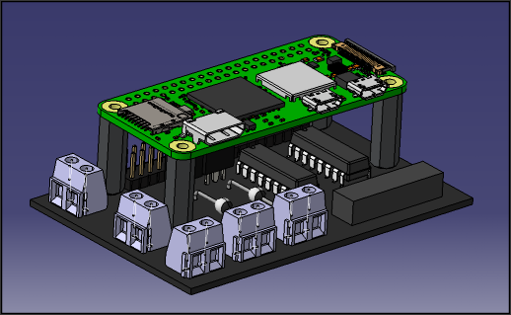
This is a model done in CATIA with M3 spacers between the Raspberry Pi and the Communication Board. The screw terminals are both for input cables, as well as outputting 12V for the Power Electronics Board.
Thermal Considerations
There hasn't been any thermal calculations or simulations done so far for this board, as it has much less power being dissipated.
High Power Board
Overview
The High Power board is the board that actually connects to the test windings.
Schematic
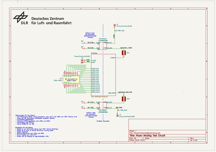
The root sheet highlights the isolation boundary as well as the electrical components that support that isolation. The following table outlines the purpose of each component at this view.
Table 2 — Component breakdown
| Component | Description / Purpose |
|---|---|
| LEV200A4ANA (DC relay) | High voltage relay. Not mounted onto the board, mounted separately. |
| 0398900302 (screw terminal) | PCB-mountable connectors for wires for connecting to external devices. |
| XG2A-1601 (IDC connector) | A PCB-mountable connector for a ribbon cable. |
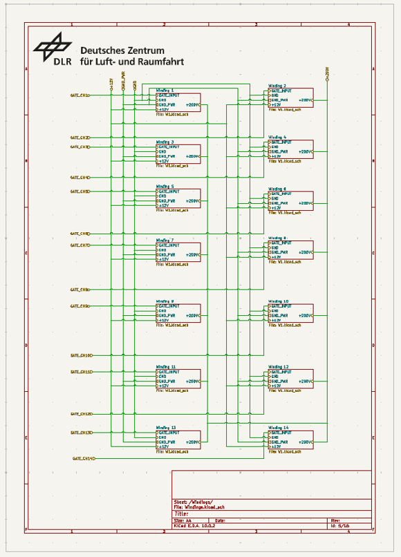
The windings sheet is mainly an intermediate sheet in order to have all fourteen windings represented on the schematic.
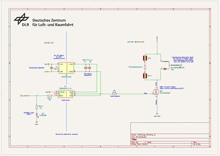
Then the individual winding schematic sheets show the flow of the board. The gate driver and DC-DC board act as the isolation boundary between the components. The gate signal triggers an LED in order for visual confirmation that each winding circuit is working as expected.
The gate driver sends a signal to the power MOSFET which runs the power through the winding. There is a freewheeling recovery diode to handle the flyback, which is the voltage spike that happens across an inductive load when a supply current is suddenly reduced.
Footprints
Routing
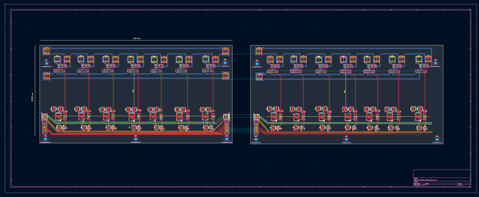
Figure 10 — Full footprint w/ routing
This is a screenshot of the full routing and component placement. It was split into two boards due to the length of the components. The choice to have all of the terminal connections to the windings on the same side is due to it being requested for the test setup. The screw terminal and ribbon cable connections are there to connect both the Communication Board to the High Power Board, as well as the two high power boards to each other.
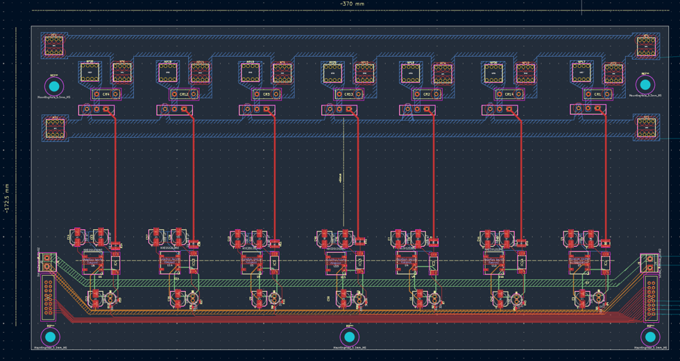
Figure 11 — Individual board with footprints and routing
The blue dashed area is a copper pour at the bottom of the board. There is also a planned copper bus bar for these areas as well, that will be laser cut.
At the bottom of the board you can see all of the logic components where the ribbon cables are. The green dashed area is an internal ground pour on the board. The sets of each winding have ground traces that connect in a circle through the components and run through the ground pour. The orange dashed area is an additional ground pour that is a +12V net, which connects each winding's set of components to it.
3D Models
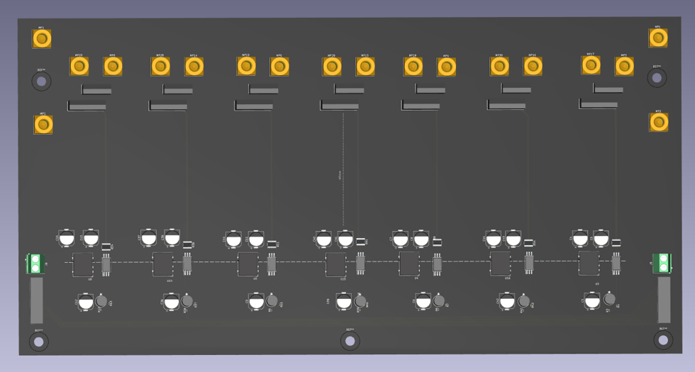
Figure 12 — KiCad 3D rendering of an individual board
The 3D model for the board. The tallest components for housing considerations are the power MOSFETs, which are tough to see in this picture.
Thermal Considerations
This board has had a lot of work going into choosing the aluminum heatsink, which is not pictured above as it had not been finalized at the time of writing. Doing a thermal simulation with Ansys is the next step for this.
Heatsink Thermal Calculation
Calculating per board: 7× IXFK240N25X3, each on for 5s, sequential (35s per run). Runs repeated back-to-back with no rest between them assumed for safety.
1. Values (for my own reference)
| Symbol | Meaning | Units | Value used |
|---|---|---|---|
| I | Drain current per device during on-time | A | 150 |
| V | Bus voltage (winding supply) | V | 200 |
| VMOSFET | Voltage drain seen by MOSFET | V | 0.75 |
| RDS(ON) | Drain-source on-resistance at a given TJ | Ω | varies |
| RDS(ON), 25°C | On-resistance at 25°C | mΩ | 5.0 |
| k(TJ) | Normalization multiplier for RDS(ON) vs. TJ (datasheet Fig. 4) | — | linear fit |
| TJ | Junction temperature | °C | X |
| TMount | Local heatsink temperature at a device's mount point at the moment it fires | °C | 25 (single-run baseline); becomes the sink's own steady-state temp under continuous duty |
| TAmbient | Ambient air temperature | °C | 25 |
| RθJC | Junction-to-case thermal resistance (datasheet) | °C/W | 0.10 |
| RθCS | Case-to-sink thermal resistance (datasheet) | °C/W | 0.15 |
| ZθJC(t) | Transient thermal impedance, junction-to-case, at pulse width t (datasheet Fig. 15) | °C/W | ≈ RθJC at t = 5s (curve has plateaued) |
| t | Single-device on-time (pulse width) | s | 5 |
| ttotal | Total on-time across all 7 devices per run | s | 35 |
| P | Power dissipated per device while on | W | ≈140 W first-run; ≈162–214 W steady-state depending on cooling |
| ΔTJ, Local | Junction temp rise above its own local mount point | °C | P × (RθJC + RθCS) |
| E | Total heat energy delivered into the shared heatsink over one 70s run | J | P × ttotal |
| m | Mass of the shared aluminum heatsink | kg | 0.672 |
| c | Specific heat of aluminum | J/(kg·K) | 897 |
| ΔTSink | Bulk heatsink temperature rise | °C | |
| h | Convection heat transfer coefficient | W/(m²·K) | 8 natural convection; ~60 forced air convection |
| Rth,sink-amb | Thermal resistance from sink to ambient air | °C/W | 1/(h×A) |
| R | Total loop resistance used in the continuous feedback solve | °C/W | R = Rth,sink-amb + 0.25 |
| ηFin | Fin efficiency | — | ~0.78 |
| kAl | Thermal conductivity of the fin material (6063-T5 extrusion) | W/(m·K) | ~200 |
2. Power Dissipation Per Device (First-Run, Cold-Start Case)
2a. Voltage drop seen by MOSFET
When the MOSFET is fully enhanced, it behaves like a resistor of value RDS(ON), therefore:
V_DS = I × R_DS(ON)
150A × 0.005Ω = 0.75V
Substituting this VDS back into P = V × I for the MOSFET specifically:
P_FET = V_DS × I
      = (R_DS(ON) × I) × I
      = I² × R_DS(ON)
2b. Power dissipation
There is a feedback loop where more power → hotter junction → higher RDS(ON) → more power → hotter junction, and it continues.
P = I² × R_DS(ON)(T_J)
Then, we can represent a linear approximation of the datasheet's Figure 4 curve (RDS(ON) normalized vs. junction temperature) with k(TJ) calibrated so k(25°C) = 1.0 and k(150°C) = 2.2, which roughly matches the shape of the curve.
Slope = (2.2 - 1.0)/(150 - 25) = 1.2/125
R_DS(ON)(T_J) = R_DS(ON), 25°C × k(T_J)
k(T_J) = R_DS(ON)(T_J) / R_DS(ON), 25°C
k(T_J) = 1.0 + (1.2/125) × (T_J - 25)
A 5-second on-time is long enough that the device heats during operation, so P and TJ are solved together, iteratively, starting from a mount baseline of TMount = 25°C:
| Iteration | TJ (°C) | k(TJ) | RDS(ON) (mΩ) | P = I² × RDS(ON) (W) |
|---|---|---|---|---|
| 0 | 25.0 | 1.000 | 5.00 | 112.5 |
| 1 | 25 + 112.5 × 0.25 = 53.1 | 1.270 | 6.35 | 142.9 |
| 2 | 25 + 142.9 × 0.25 = 60.7 | 1.343 | 6.71 | 151.0 |
| 3 | 25 + 151.0 × 0.25 = 62.75 | 1.362 | 6.81 | 153.3 |
| 4 | 25 + 153.3 × 0.25 = 63.3 | 1.368 | 6.84 | 153.9 |
| 5 | 25 + 153.9 × 0.25 = 63.5 | 1.370 | 6.85 | ≈154 (converged) |
Result: P ≈ 154 W per device, first run, ambient starting temperature.
2c. Transient thermal impedance at t = 5s
At t = 5s, the single-pulse ZθJC curve has reached its steady-state plateau (the plateau value is RθJC by definition):
Z_θJC(5s) ≈ R_θJC = 0.10 °C/W
2d. Local temperature rise (die → case → sink attach point)
ΔT_Local = P × (R_θJC + R_θCS)
ΔT_Local = 140 × (0.10 + 0.15) = 140 × 0.25 = 35 °C
This is how much hotter the junction runs above whatever the local mount point happens to be sitting at, at the moment that device begins. This is a useful reference point. It is only the mount point that changes under continuous duty.
3. Power the Cooling System Must Actually Remove (Duty Cycle → Continuous Heat Load)
Section 2 found how much power a single device dissipates while it happens to be on. This section converts the per-device number into the continuous average power the cooling system actually has to reject, which will be the value P that Section 4 carries forward into the steady-state loop.
3a. Energy per firing event
Each device firing delivers a fixed packet of energy into the sink while it's on. Using the first-run value P ≈ 154 W and t = 5s: E ≈ 154 × 5 ≈ 770 J per device, per firing.
3b. Total energy per full run
All 7 devices fire once each per run, so the total energy dumped into the shared sink over one run is:
E_total = N × P × t = P × t_total
With N = 7, t = 5s (so ttotal = 35s): Etotal ≈ 154 × 35 ≈ 5,390 J per run.
3c. Summary
| Quantity | Formula | Value (this design) |
|---|---|---|
| Energy per device firing | P × t | ≈ 770 J (first-run P) |
| Total energy per run | N × P × t | ≈ 5,390 J |
| Cycle length | ttotal + trest | 35s + 0 = 35s |
| Duty cycle | ttotal / (ttotal + trest) | 100% |
| Continuous power the sink must reject | Pavg = P × D | ≈ P ≈ 154 W first-run; ≈162–220 W steady-state |
This Pavg is the number Section 4 solves for at steady state.
4. Continuous Running Analysis
With zero rest between runs, the heatsink never returns to 25°C, but instead a different steady-state temperature. The mount temperature each device sees will be the heatsink's own running temperature, which itself depends on how much power the devices are dissipating. The power depends on RDS(ON), which depends on junction temp, which depends on mount temp. This is a closed feedback loop that I am attempting to solve with the following.
Setting up the governing equations:
Equation A (how hot the sink runs, based on power):
  T_Mount = T_Ambient + (P × R_th,sink-amb)

Equation B (junction temperature, relative to the mount):
  T_J = T_Mount + (P × (R_θJC + R_θCS)) = T_Mount + (P × 0.25)

Combining A + B:
  T_J = T_Ambient + (P × R_th,sink-amb) + (P × 0.25)
  T_J = T_Ambient + P(R_th,sink-amb + 0.25)
Let R = (Rth,sink-amb + 0.25) as the total thermal resistance from ambient to junction, so TJ = TAmbient + P·R.
Defining x and substituting the RDS(ON) feedback loop. Let x = TJ − TAmbient so the chain above becomes Equation C: x = P·R. And P itself depends on x, via a linearized self-heating relationship:
P = I² × R_DS(ON)(T_J)
R_DS(ON)(T_J) = R_DS(ON),25°C × k(T_J)
k(T_J) = 1 + 0.0096 × (T_J − 25)

Substitute x = T_J − 25:
  k = 1 + 0.0096x
  R_DS(ON) = R_DS(ON),25°C × (1 + 0.0096x)
  P = I² × R_DS(ON),25°C × (1 + 0.0096x)

Collapse the constant (I² × R_DS(ON),25°C = 150² × 0.005 = 112.5 W):
  Equation D: P = 112.5(1 + 0.0096x)
Solving the loop — substitute D into C:
x = R × 112.5 × (1 + 0.0096x)
x = 112.5R + (112.5 × 0.0096)Rx
x = 112.5R + 1.08Rx
x − 1.08Rx = 112.5R
x(1 − 1.08R) = 112.5R
x = 112.5R / (1 − 1.08R),  where R = R_th,sink-amb + 0.25
Note: this equation has a ceiling of R ≥ 0.926 °C/W.
Solving for the sink-to-ambient thermal resistance needed to hold a given steady-state TJ target under continuous duty:
| Target TJ (°C) | Required R (total) °C/W | Required Rth,sink-amb °C/W | Steady-state P (W) |
|---|---|---|---|
| 100 (x = 75) | 0.388 | 0.138 | 193.5 |
| 110 (x = 85) | 0.416 | 0.166 | 204.3 |
| 125 (x = 100) | 0.454 | 0.204 | 220.5 |
| 150 (absolute ceiling) (x = 125) | 0.505 | 0.255 | 247.5 |
5. Proposed Heatsink
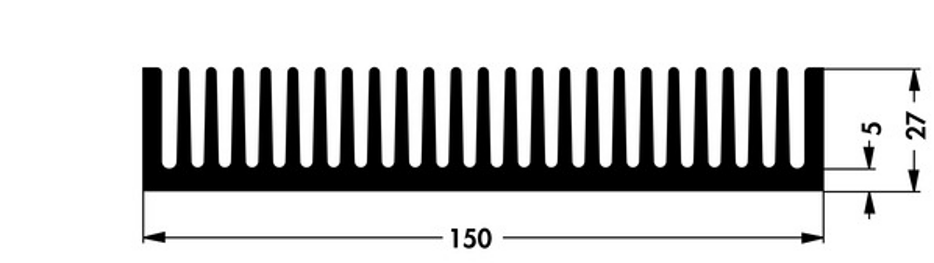
Starting search dimensions: 300 mm long × 30 mm wide × 50 mm tall. 2 × 150mm wide, 50mm long, 27mm tall is the chosen option, placed edge to edge.
5a. Design candidate
| Parameter | Value |
|---|---|
| Part | Fischer SK 58 100 SA, cut to 50mm |
| Material | Aluminium 6063-T5 |
| Width × height | 150 mm × 27 mm |
| Length (cut) | 50 mm |
| Base plate thickness | 5 mm |
| Fin height above base | 22 mm |
| Fin count | 23 |
| Fin thickness | ≈ 3.0 mm |
| Edge wall thickness | 5.0 mm |
| Fin pitch / gap | ≈ 3.0 mm |
| Thermal conductivity, kAl | 200 W/(m·K) |
| Sink mass (50 mm cut) | ≈ 336 g |
5b. Fin efficiency and effective area
Shared geometry:
L     = extrusion length (cut length)   = 0.050 m
L_f   = fin height above base           = 0.022 m
k_Al  = thermal conductivity            = 200 W/(m·K)
b_fin = fin thickness (assumed)         = 0.003 m  (×23)
b_edge= edge wall thickness (assumed)   = 0.005 m  (×2)
Legend:
P      = wetted perimeter of fin/edge cross-section = 2(b+L), m
A_c    = cross-sectional area = b × L, m²
m      = fin parameter = √(h × P / (k_Al × A_c)), m⁻¹
L_c    = corrected height = L_f + b/2, m (accounts for tip losses)
η      = fin efficiency = tanh(m·L_c) / (m·L_c)
Total sink mass:
A_Cross = (150×5) + (23×3.0×22) + (2×5.0×22)
        = 750 + 1518 + 220 = 2488 mm²
m_sink  = ρ_Al × A_cross × L = 2700 × 2.488e-3 × 0.050 = 0.336 kg
m_combined = 2 × 0.336 = 0.672 kg
Case 1: Natural convection, h = 8 W/m²·K
Regular fins (×23, b = 0.003m)
  P_fin   = 2 × (0.003 + 0.050) = 0.1060 m
  A_c,fin = 0.003 × 0.050 = 1.50e-4 m²
  m       = √(8 × 0.1060 / (200 × 1.50e-4)) = √(28.27) = 5.317 m⁻¹
  L_c,fin = 0.022 + 0.003/2 = 0.0235 m
  m·L_c   = 5.317 × 0.0235 = 0.1249
  η_fin   = tanh(0.1249)/0.1249 = 0.9948

Edge walls (×2, b = 0.005m)
  P_edge   = 2 × (0.0050 + 0.050) = 0.1100 m
  A_c,edge = 0.0050 × 0.050 = 2.50e-4 m²
  m_edge   = √(8 × 0.1100 / (200 × 2.50e-4)) = √(17.60) = 4.195 m⁻¹
  L_c,edge = 0.022 + 0.0050/2 = 0.02450 m
  m·L_c    = 4.195 × 0.02450 = 0.1028
  η_edge   = tanh(0.1028)/0.1028 = 0.9965

Areas
  A_fins,total   = 23 × (2 × 0.02350 × 0.050) = 54050 mm²
  A_edges,total  = 2  × (2 × 0.02450 × 0.050) = 4900 mm²
  A_base,exposed = (150×50) − (23×3.0 + 2×5.0)×50 = 3550 mm²
  A_eff = 0.9948×54050 + 0.9965×4900 + 3550
        = 53768 + 4883 + 3550 = 62203 mm² = 0.0622 m²
  A_eff,combined = 2 × 0.0622 = 0.1244 m²

Thermal resistance
  R_th,sink-amb = 1/(8 × 0.1244) = 1.005 °C/W

Steady-state loop
  R_total = 1.005 + 0.25 = 1.255 °C/W

Testing stability
  R_total < 1/1.08 (0.9259)?
  1.255 < 0.9259  →  NOT TRUE
Therefore, the system doesn't reach a steady state with natural cooling, and would break down.
Transient time to TJ = 150°C from ambient start, where y = TMount − TAmbient:
- Term 1: msink·c·(dy/dt) — the heatsink's heat capacity multiplied by the rate of change of the temperature difference.
- Term 2: P(x(y)), where P(x) = 112.5 × (1 + 0.0096x) — the MOSFET dissipates more heat as the junction gets hotter because RDS(ON) increases with temperature.
- Term 3: y / Rth,sink-amb — heat leaving per second, represented by temperature rise divided by thermal resistance.
m_sink × c × (dy/dt) = P(x(y)) − (y / R_th,sink-amb)
0.672 × 897 × (dy/dt) = P(x(y)) − (y / R_th,sink-amb)
602.9 × (dy/dt)       = P(x(y)) − (y / R_th,sink-amb)

x(y) = y + 0.25 × P(x)
x(y) = y + 28.125 + 0.27x
0.73 x(y) = y + 28.125
x(y) = (y + 28.125) / 0.73
P(x) = 112.5 × (1 + 0.0096x)
Solution method — the governing equation is a first-order ODE with the power term P(x(y)) depending on y itself (through x), so it cannot be solved in one algebraic step. Instead it is solved by numerical (step-by-step) integration, evaluated in the following order at each timestep:
- Given the current sink temperature y, compute the junction temperature: x = (y + 28.125) / 0.73
- Given x, compute the power currently being dissipated: P(x) = 112.5 × (1 + 0.0096x)
- Compute the heat currently leaving through the sink: Qout = y / Rth,sink-amb
- Compute the instantaneous rate of change of sink temperature: dy/dt = [P(x) − Qout] / (msink·c)
- Advance y forward by one small timestep dt: y(t+dt) = y(t) + (dy/dt)·dt
- Repeat steps 1–5, starting from y(0) = 0 (sink at ambient), until x ≥ 125 (i.e. TJ = 150°C).
This is necessary because P depends on x, x depends on y, and y's rate of change depends on P. This was done with an online ODE calculator.
Result: TJ crosses 150°C at t = 225s. Therefore, the system could be run through 6 cycles without active cooling with this heatsink setup.
Case 2: Forced air, h = 60 W/m²·K
Regular fins (×23, b = 0.003m)
  P_fin   = 2 × (0.003 + 0.050) = 0.1060 m
  A_c,fin = 0.003 × 0.050 = 1.50e-4 m²
  m       = √(60 × 0.1060 / (200 × 1.50e-4)) = √(212.0) = 14.56 m⁻¹
  L_c,fin = 0.022 + 0.003/2 = 0.0235 m
  m·L_c   = 14.56 × 0.0235 = 0.3422
  η_fin   = tanh(0.3422)/0.3422 = 0.9627

Edge walls (×2, b = 0.005m)
  P_edge   = 2 × (0.0050 + 0.050) = 0.1100 m
  A_c,edge = 0.0050 × 0.050 = 2.50e-4 m²
  m_edge   = √(60 × 0.1100 / (200 × 2.50e-4)) = √(132.0) = 11.49 m⁻¹
  L_c,edge = 0.022 + 0.0050/2 = 0.02450 m
  m·L_c    = 11.49 × 0.02450 = 0.2815
  η_edge   = tanh(0.2815)/0.2815 = 0.9744

Areas
  A_fins,total   = 23 × (2 × 0.0235 × 0.050) = 54050 mm²
  A_edges,total  = 2 × (2 × 0.02450 × 0.050) = 4900 mm²
  A_base,exposed = (150×50) − (23×3.0 + 2×5.0)×50 = 3550 mm²
  A_eff = 0.9627×54050 + 0.9744×4900 + 3550
        = 52037 + 4775 + 3550 = 60359 mm² = 0.0604 m²
  A_eff,combined = 0.1207 m²

Thermal resistance
  R_th,sink-amb = 1/(60 × 0.1207) = 0.138 °C/W

Steady-state loop
  R_total = 0.138 + 0.25 = 0.388 °C/W

Testing stability
  R_total < 1/1.08 (0.9259)?
  0.388 < 0.9259  →  TRUE
Yes, therefore the system does reach a steady state with forced air cooling.
x = 112.5 × 0.388 / (1 − 1.08 × 0.388) = 43.65 / 0.581 = 75.2
T_J,steady-state = 25 + 75.2 = 100.2 °C
Well within the 150°C temperature rating of the MOSFET.
P_steady-state = 112.5 × (1 + 0.0096 × 75.2) = 193.7 W
Transient time to TJ = 100.2°C from ambient start follows the same process as h = 8:
m_sink × c × (dy/dt) = P(x(y)) − (y / R_th,sink-amb)
602.9 × (dy/dt) = P(x(y)) − (y / R_th,sink-amb)
x(y) = (y + 28.125) / 0.73
P(x) = 112.5 × (1 + 0.0096x)
Result: TJ approaches 100.2°C at t = 377s (~6.3 min, 10.8 cycles). It never crosses 150°C (theoretically).
6. Fan Sizing
6a. Channel geometry (flow path)
Channel cross-section = fin height × gap
  0.022m × 0.003m = 66 mm² (per channel)
Free-flow area = 48 channels × 66 mm²
  = 3168 mm² = 3.168e-3 m²
6b. Velocity needed to hit h = 60 W/m²·K
To solve for this, I'm using the Blasius/Pohlhausen formula for laminar boundary-layer flow over a flat plate, averaged over the plate length:
Nu_L = 0.664 × Re_L^0.5 × Pr^(1/3)
- Nu (Nusselt number) represents how much better convection is, compared to if the air was stagnant.
- Re (Reynolds number) represents how turbulent the airflow is.
- Pr (Prandtl number) is a property of fluids, comparing how fast momentum diffuses vs. how fast heat diffuses through the fluid. 0.70 is the value for air.
Turning the Nusselt number into a target using its definition:
Nu = h × L / k_air
Nu_L = 60 × 0.050 / 0.0280 = 107.1
Subbing in values:
Nu_L = 0.664 × Re_L^0.5 × Pr^(1/3)
Re_L^0.5 = Nu_L / (0.664 × Pr^(1/3))
Re_L^0.5 = 107.1 / (0.664 × 0.888)
Re_L^0.5 = 107.1 / 0.590 = 181.7
Re_L = 33,026
Then using the definition of Reynolds number, we solve for velocity:
Re_L = V × L / ν_air
V = 33,026 × 1.80e-5 / 0.050 = 11.9 m/s
6c. Converting to volumetric flow (CFM)
Q_vol = V × A_freeflow = 11.9 m/s × 3.168e-3 m² = 0.0377 m³/s
CFM   = Q_vol × 2118.88 = 79.8 CFM
Therefore, using a fan or fans with a rating of 100 CFM free air in order to account for any derating should be able to successfully cool the devices for continuous testing.
6d. Possible fan suggestion
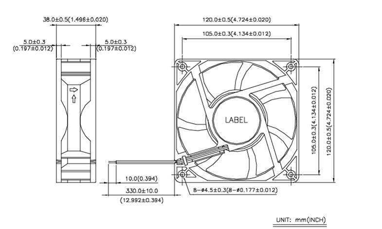
3 × AFB1212HE fans to handle both boards. Rated for 12V. Each rated for 105.94 CFM. Rated for 41.0 dB, so also quiet.
7. Summary
| Scenario | Cooling | Steady-state P | Steady-state / worst-case TJ |
|---|---|---|---|
| Single 35s run, full rest before repeat | Base aluminum blocks | ≈ 154 W | ≈ 63.5 °C |
| No-rest, natural convection | Natural convection, aluminum block | ≈ 154 W initially, then rises without bound | Reaches 150 °C in ≈366s (≈6.1 min) |
| No-rest, finned sink + forced air | 2× SK58 100 SA (cut to 50mm, mounted side-by-side) + ~100 CFM fan | ≈ 193.7 W | ≈ 100.2 °C steady-state |